
1.Metasurfaces & Metalenses
Core flat-optic and wavefront-control family spanning compact beam shaping, imaging and structured interfaces.
Open Topic →Planar subwavelength surfaces and flat-optic architectures for beam steering, imaging, filtering and compact photonic / RF system integration.
Core flat-optic and wavefront-control family spanning compact beam shaping, imaging and structured interfaces.
Open Topic →
Large-area metasurface apertures for compact lenses, holography, steering and thin optical subsystems.
Open Topic →
Low-profile structured surfaces enabling scanning, coupling efficiency and compact communication payloads.
Open Topic →
Reconfigurable skins using programmable, MEMS or phase-change control for adaptive response in service.
Open Topic →
Phase-gradient and impedance-engineered surfaces for shaping amplitude, phase and polarization.
Open Topic →
Dielectric, plasmonic and hybrid nanostructure platforms for flat optics and advanced coupling behavior.
Open Topic →
Beam steering, acoustic cloaks and high-efficiency dielectric metalens developments tracked for maturity lift.
Open Topic →
Use the canonical family view to keep optical, RF, fabrication and qualification decisions aligned.
Open Topic →| Material / Subfamily | Primary Engineering Functions | Environment / Interfaces | Processing / Qualification Focus | Cross-Project Links |
|---|---|---|---|---|
| Electromagnetic Metasurfaces | Beam-steering, impedance-engineered RF surfaces for compact apertures, filters and field shaping. | Backplane conductors, dielectric loss, radome integration, thermal drift and power handling constrain architecture. | Full-wave correlation, angle response, insertion loss, array uniformity and chamber/range verification are central. | Communications · Portal Field · Sensors |
| Optical Metasurfaces | Subwavelength optical phase, amplitude and polarization control in very thin form factors. | Substrate cleanliness, spectral band, thermal load, contamination and package alignment strongly affect output. | Nanopattern fidelity, spectral metrology, polarization mapping and environmental stability screening govern release. | Sensors · Medical · Computing |
| Metalenses | Flat-optic focusing and imaging structures for compact cameras, biosensors and photonic payloads. | Chromatic aberration, NA, working distance, package stack-up and contamination control bound usable performance. | MTF characterization, spectral response, wafer uniformity, shock/thermal testing and assembly tolerance dominate. | Medical · Sensors · Space Propulsion |
| Tunable / Active Surfaces | Reconfigurable surfaces driven by MEMS, liquid crystal, phase-change or electronic control layers. | Drive electronics, cycling fatigue, hysteresis, switching heat and calibration drift become first-order interfaces. | Response time, actuation endurance, tuning range, repeatability and feedback-control calibration require qualification. | Communications · Portal Field · Prototype Qualification |
| Dielectric Nanostructures | Low-loss dielectric nanoresonators enabling efficient wavefront shaping, filtering and spectral selectivity. | Index control, substrate compatibility, CTE mismatch and contamination govern stability and performance. | Etch profile control, sidewall roughness, spectral verification and package cleanliness are key process gates. | Crystals & Electronic Materials · Communications |
| Plasmonic / Conductive Surfaces | Conductive, plasmonic and hybrid surfaces for extreme field confinement, coupling and compact interfaces. | Ohmic loss, oxidation, surface roughness, electromigration and thermal flux limit usable envelopes. | Thin-film control, adhesion, nanoscale metrology, drift monitoring and coupling-efficiency tests dominate. | Nanotechnology · Sensors · Computing |
| Nonlinear & Quantum-Adjacent Optics | Engineered interfaces supporting nonlinear mixing, switching and emerging photonic / quantum-adjacent functions. | Pump intensity, thermal stability, coherence sensitivity, packaging and material purity become decisive. | Nonlinear response mapping, stability over cycling, spectral purity and interface loss must be verified. | Crystals & Electronic Materials · Prototype Qualification |
RF front ends, beam steering, compact apertures and adaptive wave-control surfaces.
Explore →
Flat optics, modulation, compact imaging stacks and integrated photonic functions.
Explore →
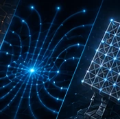
Structured-interface concepts for field shaping, coupling and beam manipulation.
Explore →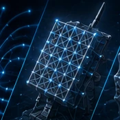
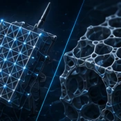
Nanofabrication, overlay control, alignment, metrology and qualification workflow.
Explore →