1.2D Materials
Graphene, MXenes and other atomically thin material families for electrical, thermal, barrier and sensing functions.
Open Topic →Nanoscale materials, structures, interfaces, devices, metrology and manufacturing pathways that cut across every major Materials Engineering family.
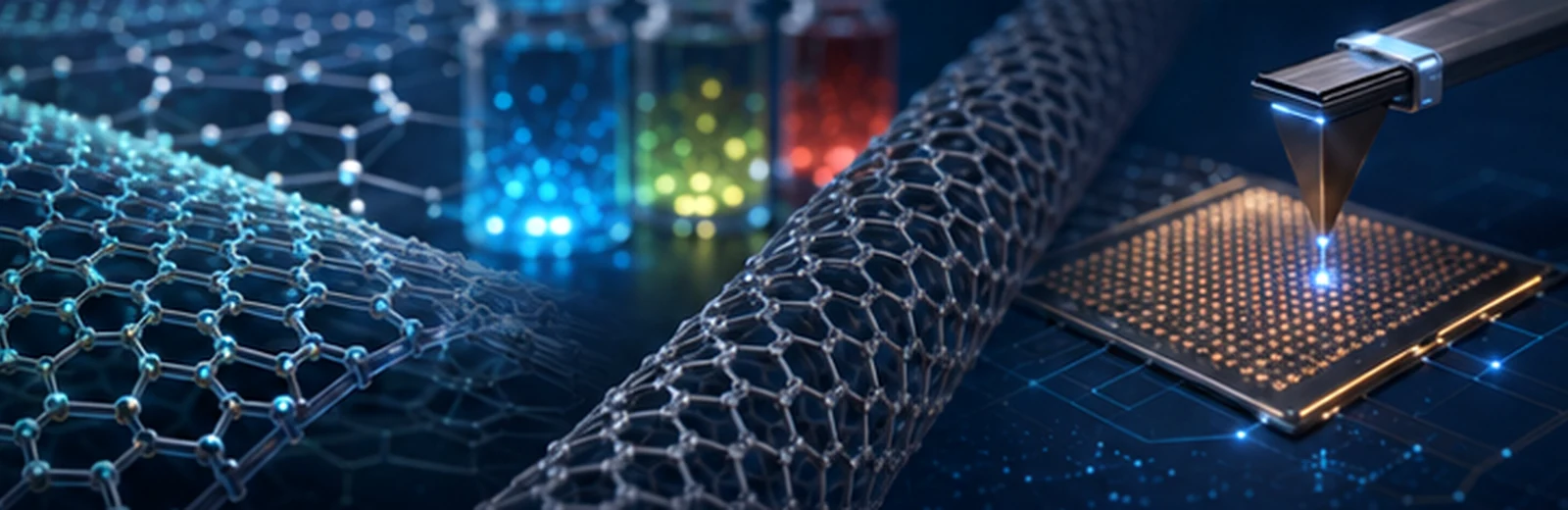
Graphene, MXenes and other atomically thin material families for electrical, thermal, barrier and sensing functions.
Open Topic →
Carbon and boron-nitride nanotube architectures for reinforcement, transport, field emission and nanoelectronic systems.
Open Topic →
Tailorable nanoscale dimensions for catalysts, electronics, filtration, reinforcement, delivery and sensing systems.
Open Topic →
Size-dependent optical and electronic nanostructures for emission, detection, conversion and quantum-enabled devices.
Open Topic →
Nanoscale reinforcement and multifunctional matrices combining structural, thermal, electrical and barrier functions.
Open Topic →
High-surface-area porous structures for insulation, adsorption, catalytic support, filtration and energy functions.
Open Topic →
Nanoscale devices, contacts and transducers for sensing, computing, memory and integrated optoelectronic systems.
Open Topic →
Light-matter interaction at the nanoscale for waveguides, resonant surfaces, sensors and compact photonic systems.
Open Topic →
Controlled synthesis, patterning, deposition, inspection, characterization and scale-up for nanoscale systems.
Open Topic →| Material / Subfamily | Primary Engineering Functions | Environment / Interface Risks | Processing / Qualification Focus | Cross-Project Links |
|---|---|---|---|---|
| 2D Materials | Electrical and thermal transport, barrier layers, sensing and functional surfaces. | Defects, transfer contamination, substrate coupling and interface chemistry can dominate performance. | Growth or exfoliation route, transfer control, thickness, defects, contacts and characterization. | Library · Selection · Electronics · Thermal |
| CNT & BNNT | Reinforcement, conduction or insulation pathways, field emission and thermal transport. | Alignment, dispersion, interfacial load transfer, oxidation and contact resistance are configuration-dependent. | Growth, purification, dispersion, alignment, joining and repeatable property verification. | Composites · Space · Energy · Sensors |
| Nanoparticles, Nanowires & Nanofibers | Catalysis, transduction, reinforcement, filtration and tailored electrical/optical response. | Agglomeration, surface chemistry, contamination and morphology changes can alter system behavior. | Particle-size distribution, morphology, surface treatment, dispersion, handling and process repeatability. | Biomaterials · Sustainability · Sensors · Manufacturing |
| Quantum Dots & Nanocrystals | Emission, detection, conversion, imaging and size-tunable electronic/optical response. | Surface states, ligand stability, oxidation, thermal exposure and size distribution require control. | Synthesis, passivation, composition, size distribution, encapsulation and device integration. | Crystals · Photonics · Computing · Medical |
| Nanocomposites | Multifunctional structural, conductive, thermal, barrier and sensing material systems. | Dispersion, percolation, filler/matrix interfaces and anisotropy can control realized properties. | Mixing, infiltration, cure or consolidation route, interface control, scale-up and lot variability. | Composites · Aerospace · Energy · Infrastructure |
| Nanoporous Materials & Aerogels | Thermal insulation, adsorption, filtration, catalysis and high-surface-area energy functions. | Pore collapse, moisture, contamination, dusting and mechanical fragility are use-case dependent. | Gelation or templating, drying, pore architecture, reinforcement, sealing and pore metrology. | Aerogels · Thermal · Water · Space |
| Nanoelectronics & Sensors | Transistors, memory, interconnects and electrical, optical, chemical or biological transduction. | Contacts, thermal load, electromigration, drift, contamination and package interfaces affect reliability. | Lithography, deposition, etch, contacts, calibration, packaging, repeatability and aging tests. | Computing · Communications · Medical · QFL |
| Nanophotonics & Plasmonics | Wave control, resonance, enhanced light-matter interaction, sensing and compact optical functions. | Surface roughness, optical loss, thermal loading, geometry tolerance and environmental contamination matter. | Patterning, deposition, dimensional metrology, optical characterization and system integration. | Metasurfaces · Crystals · Sensors · Communications |
| Nanomanufacturing & Metrology | Repeatable nanoscale synthesis, patterning, inspection and process control. | Cleanliness, tool limits, drift, sampling strategy and statistical process variation can dominate yield. | Process windows, calibration, traceability, inline metrology, defect control and scale-up readiness. | Manufacturing · Qualification · Library · All Programs |

Electrodes, interfaces, transport pathways and high-surface-area architectures.
Explore →