Semiconductor Fabrication & Process Engineering
Wafer processing, lithography, deposition, etch, implantation, diffusion, CMP, metrology, contamination and yield.
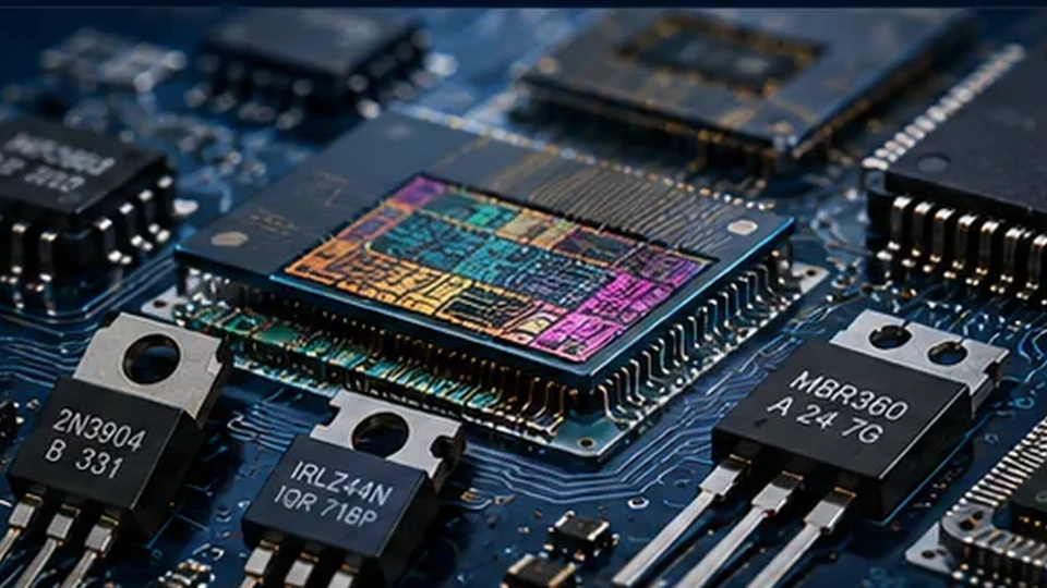
Map the controlled sequence that turns a starting wafer into patterned, doped, interconnected and tested semiconductor devices.
Technical coverage
The Level-2 index stays readable; depth moves into focused Level-3 technical pages with their own diagrams, documents and source assignments.
Wafer Materials & Preparation
Starting wafers, crystal quality, slicing, polishing, cleaning, surface preparation and incoming-material controls.
Open technical route →
Photolithography & Patterning
Photoresist, exposure, masks, alignment, resolution, pattern transfer and the dimensional control behind device features.
Open technical route →
Deposition & Epitaxy
CVD, PVD, ALD, epitaxial growth and thin-film control for conductors, dielectrics and semiconductor layers.
Open technical route →
Etch & Plasma Processes
Wet and dry etching, plasma chemistry, anisotropy, selectivity, profile control and process-induced damage.
Open technical route →
Doping, Implant & Diffusion
Ion implantation, diffusion, activation and thermal processing used to form controlled electrical regions.
Open technical route →
CMP, Metrology & Yield
Planarization, dimensional metrology, defect inspection, statistical process control and yield-learning feedback.
Open technical route →Documentation lanes
Public-facing knowledge is separated from internal engineering control and source-library notes.
Related Electrical Engineering Systems
These categories share interfaces, constraints or technology dependencies with this subject.