Documentation lane
Design Guides
Applied design guidance will be published here after source audit and technical review. The initial route map is already in place.
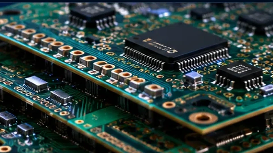
PCB
PCB Design Workflow
Architecture, schematic, placement, routing, DFM and release flow.
SI/PI
Signal & Power Integrity
Channel, PDN, grounding, EMC and ESD review workflow.
PWR
Power Conversion
Topology, component, layout, thermal and protection design sequence.
RF
RF / Microwave
High-frequency partitioning, matching, layout and measurement workflow.
PKG
Packaging & Thermal
Package, board, thermal path and mechanical integration workflow.
TEST
Manufacturing & Test
DFM/DFA, test-access, inspection, validation and reliability flow.