3D & Heterogeneous Integration
Chiplets, interposers, hybrid bonding, TSVs, redistribution layers, memory-on-logic and multi-technology system integration.
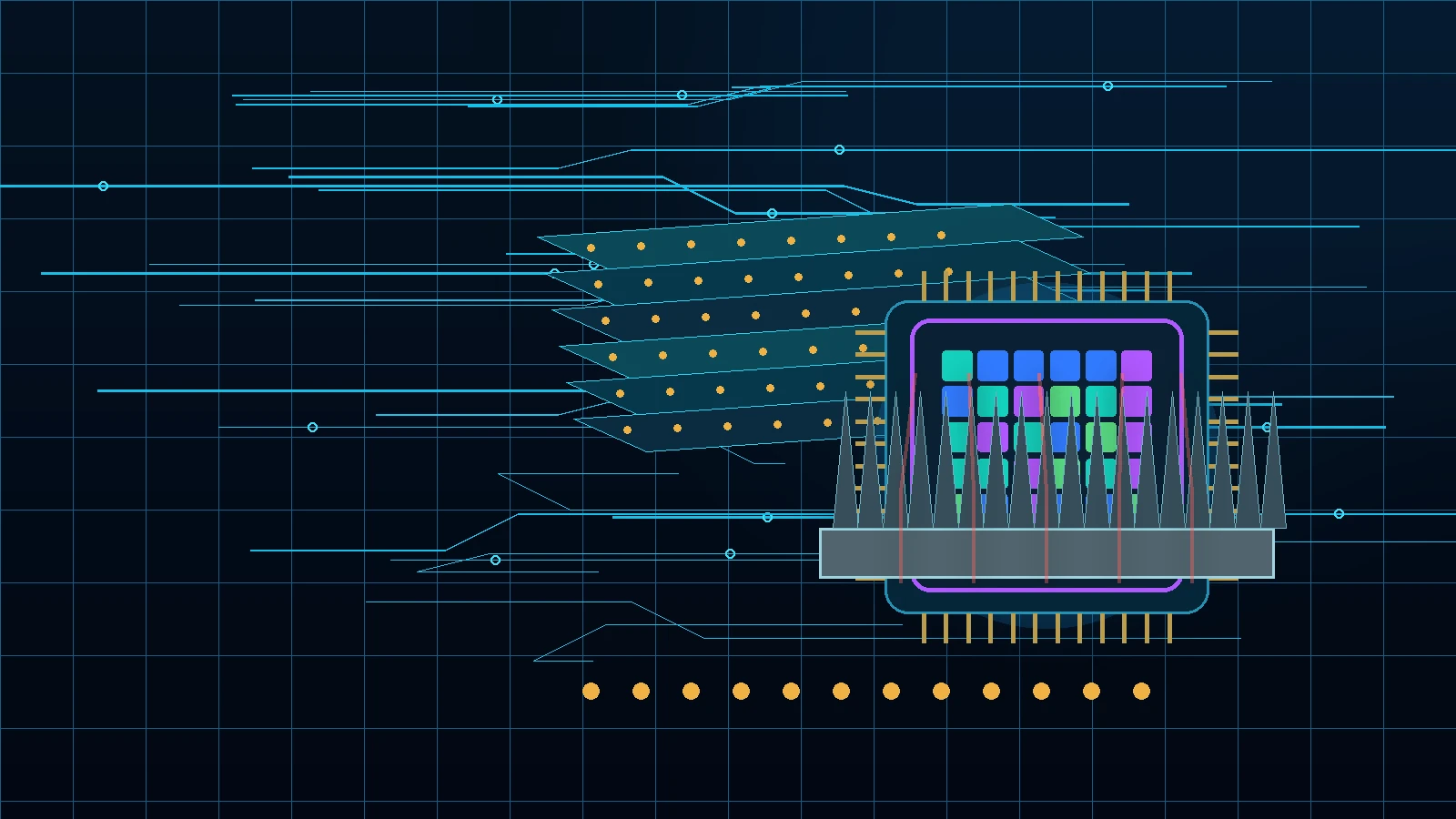
Move beyond a monolithic-chip view and engineer the package as a system: partitioning, interconnect density, power delivery, thermal paths, test, yield and technology mixing.
Architecture is stable; technology maturity is not assumed. Public claims are anchored to current authoritative sources and are separated from Aurora concept work.
Technical coverage
Six focused routes keep device physics, interfaces, packaging, controls and verification separable.
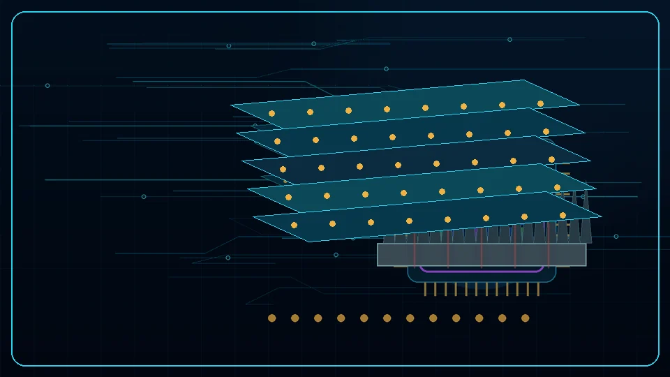
Chiplet Partitioning
Functional decomposition, die reuse, yield and interface ownership.
Open technical route →
Interposers & RDL
Silicon/organic interposers, redistribution layers and routing density.
Open technical route →
Hybrid Bonding
Die-to-wafer and wafer-to-wafer bonding, fine-pitch Cu interconnect and alignment.
Open technical route →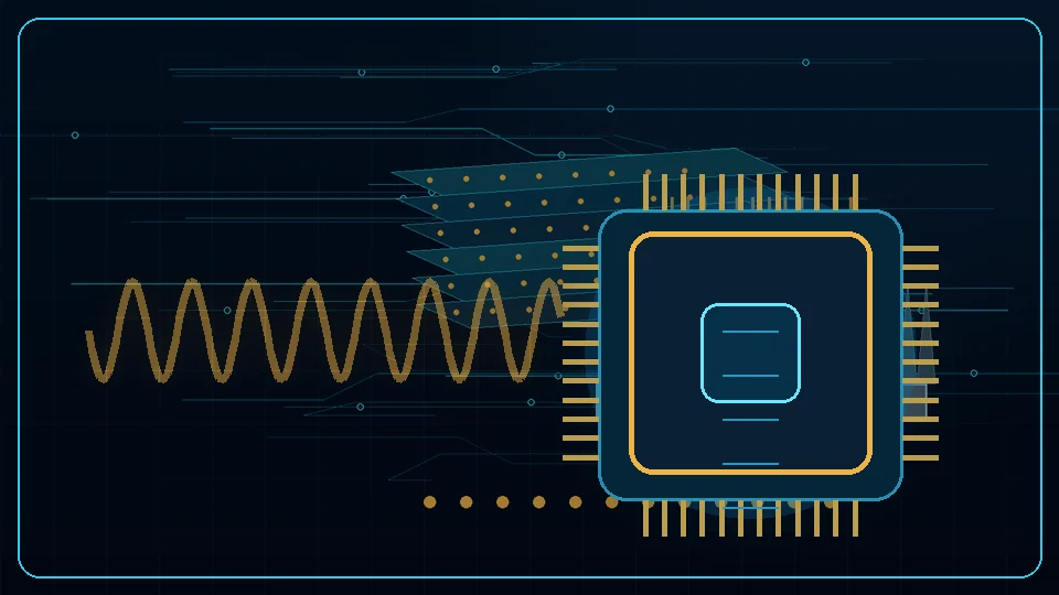
TSVs & Vertical Interconnect
Through-silicon vias, microbumps, vertical power/signal routing and parasitics.
Open technical route →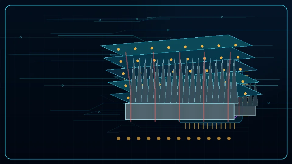
Thermal & Power Delivery
Hotspot coupling, backside power, package impedance and cooling.
Open technical route →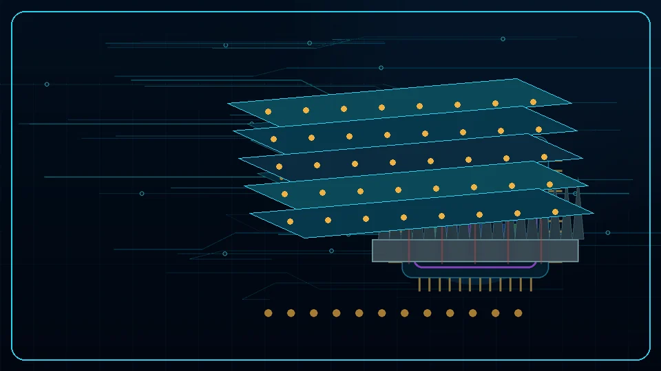
Known-Good Die & Test
Pre-bond test, repair/redundancy, yield stacking and post-bond observability.
Open technical route →3D & Heterogeneous Integration system view
Move beyond a monolithic-chip view and engineer the package as a system: partitioning, interconnect density, power delivery, thermal paths, test, yield and technology mixing.