Cryogenic Electronics
Semiconductor, analog, RF, digital, packaging and interconnect behavior at cryogenic temperatures for quantum, sensing, space and scientific systems.

Treat temperature as a first-class electrical design variable: device models shift, passive behavior changes, materials contract and every wire becomes a thermal path.
Architecture is stable; technology maturity is not assumed. Public claims are anchored to current authoritative sources and are separated from Aurora concept work.
Technical coverage
Six focused routes keep device physics, interfaces, packaging, controls and verification separable.
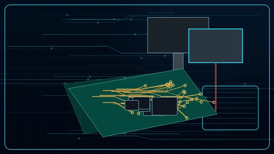
Cryo-CMOS
MOS device behavior, model validity, biasing and integrated control at low temperature.
Open technical route →
Low-Noise Amplification
Cryogenic LNAs, noise temperature, gain and placement tradeoffs.
Open technical route →
Passives & Materials
Capacitors, resistors, dielectrics, magnetics and material-property shifts.
Open technical route →
Thermal Load & Wiring
Cable heat leaks, thermalization, attenuation and stage-to-stage routing.
Open technical route →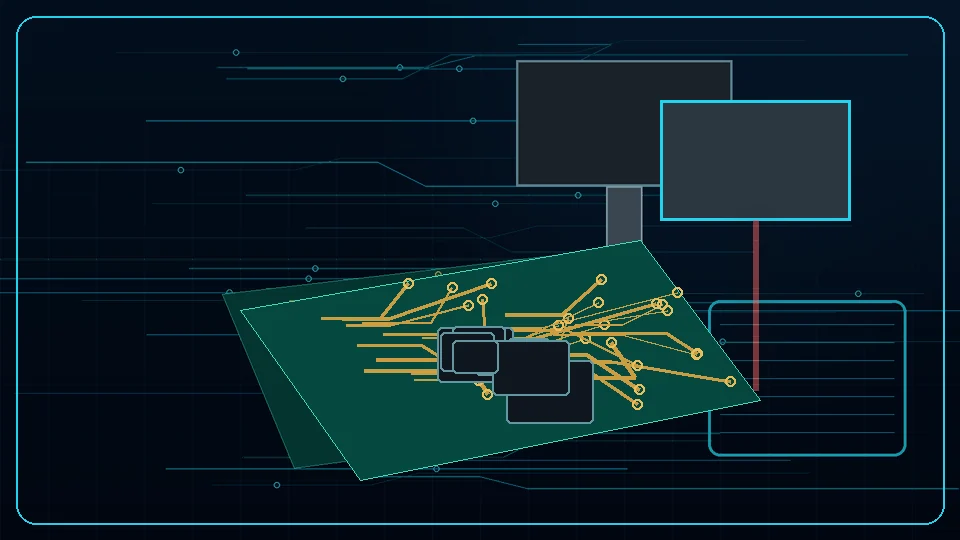
Cryogenic Connectors & Packaging
Differential contraction, seals, connectors, flex and mechanical interfaces.
Open technical route →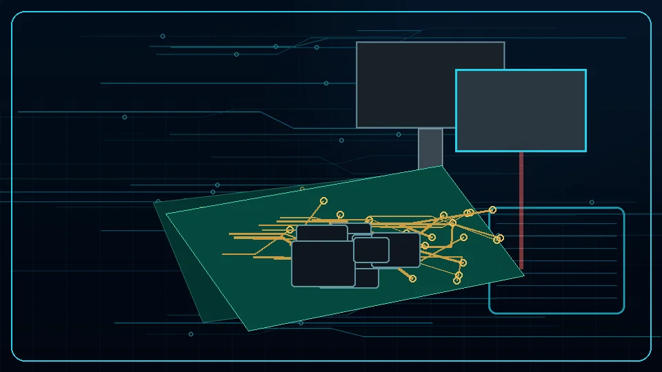
Verification & Calibration
Temperature cycling, calibration stability, drift and low-temperature test methodology.
Open technical route →Cryogenic Electronics system view
Treat temperature as a first-class electrical design variable: device models shift, passive behavior changes, materials contract and every wire becomes a thermal path.