PCB Architecture & Design
From concept to manufacturable reality: rigid, multilayer, HDI, flex and rigid-flex architecture; stackups, vias, routing, grounding and design-control workflow.
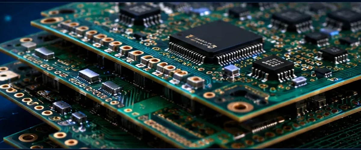
Explore PCB Design Topics
The gold-master visual structure is now implemented as native HTML with individually integrated WebP graphics.

Rigid PCBs
Fundamentals, materials, and standard board designs.
Open route →
Multilayer Boards
Layer-stack architecture, planes, dielectrics and high-density board construction.
Open route →
HDI & Microvias
Microvias, buildup structures and density-driven interconnect design.
Open route →
Flex Circuits
Flexible substrates, bend regions and dynamic interconnect constraints.
Open route →
Rigid-Flex PCBs
Rigid and flexible zones integrated into a single board architecture.
Open route →
Stackups & Layering
Layer order, copper weights, reference planes and dielectric selection.
Open route →
Vias & Interconnects
Through, blind, buried and microvia strategy with manufacturability controls.
Open route →
Routing & Layout
Placement-aware routing, differential structures and return-path continuity.
Open route →
Grounding & Shielding
Reference structures, current return paths, partitioning and EMC control.
Open route →
Design Workflow
Schematic intent through layout review, DFM and controlled release.
Open route →Stackup & Layering
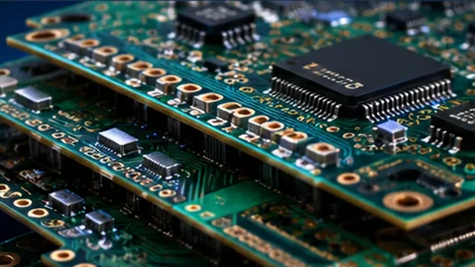
Layer sequencing, reference planes, copper distribution and dielectric selection are treated as an electrical, mechanical and manufacturing system—not an afterthought.
Via-in-Pad & High-Density Interconnect
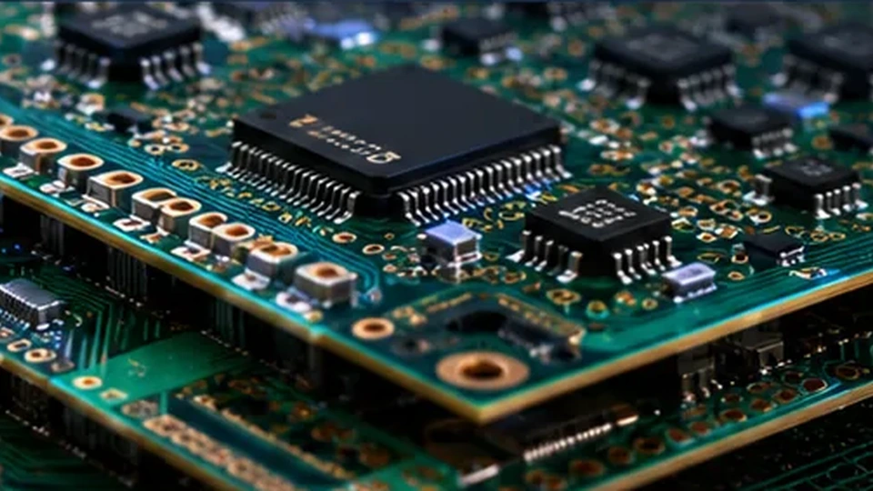
Via technology is selected around routing density, current path, signal integrity, fabrication capability, reliability and inspection requirements.
Design around the interfaces
Board architecture closes only when electrical intent, physical stackup, fabrication rules and validation requirements agree.